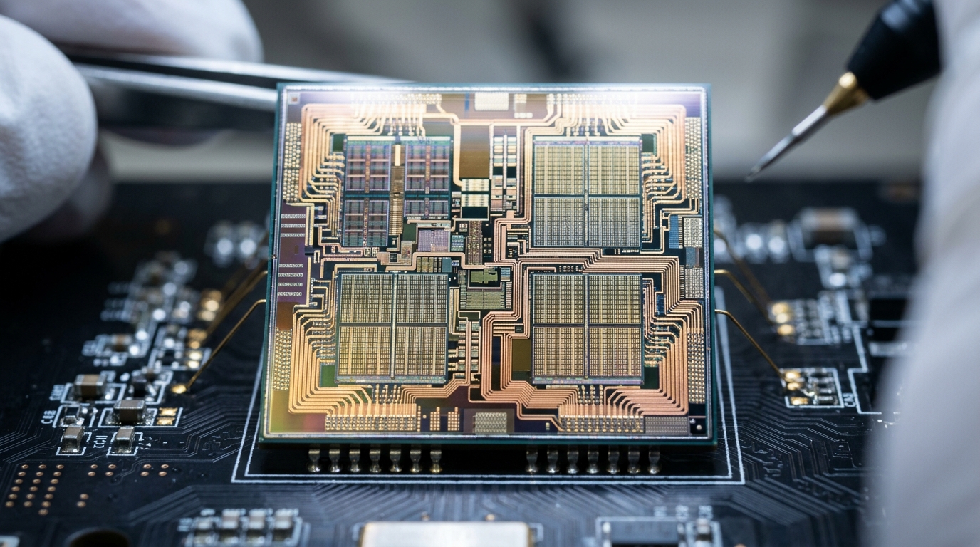
In modern computer systems, the central processing unit (CPU) can execute billions of instructions per second. A modern processor core clocked at 4.5 GHz executes a clock cycle every 0.22 nanoseconds. However, accessing data from main system memory (Dynamic Random-Access Memory, or DRAM) typically takes between 50 and 100 nanoseconds—equivalent to hundreds of wasted CPU cycles where the execution pipeline sits completely idle.
This fundamental performance disparity is known in computer architecture as the Memory Wall. To prevent processors from starving for data, chip architects place small, extremely fast pools of static memory directly onto the processor die. This specialized memory is called Cache Memory.
What is Cache Memory?
Cache memory is a high-speed volatile memory bank positioned physically adjacent to or integrated directly into the CPU cores. Its primary job is to store temporary copies of frequently used instructions and data blocks so the CPU can retrieve them in single-digit clock cycles rather than reaching across the motherboard bus to main RAM.
Unlike main memory (DRAM), which uses a single transistor and capacitor per bit and requires periodic electrical refreshing, cache memory is constructed from Static RAM (SRAM). SRAM utilizes a multi-transistor flip-flop circuit (typically 6 transistors per memory cell). Because SRAM does not require capacitive refreshing, it operates at lightning-fast switching speeds, making it the fastest memory tier in a computer outside of the processor's internal architectural registers.
The Computer Memory Hierarchy
Computer memory is organized as a pyramid reflecting the trade-offs between speed, physical footprint, thermal dissipation, and monetary cost per bit:
- CPU Registers: 0.2–0.5 nanoseconds latency (tens of bytes, zero wait states).
- Level 1 (L1) Cache: 0.8–1.5 nanoseconds latency (tens to hundreds of kilobytes, per-core).
- Level 2 (L2) Cache: 3–7 nanoseconds latency (hundreds of kilobytes to several megabytes, per-core).
- Level 3 (L3) Cache: 10–25 nanoseconds latency (tens to hundreds of megabytes, shared across cores).
- Main Memory (DRAM): 50–100 nanoseconds latency (gigabytes to terabytes).
- Non-Volatile Storage (NVMe SSD / Flash): 10,000–50,000 nanoseconds (terabytes).
- Mechanical Storage / Cold Archive: Millions of nanoseconds.
The Three Levels of CPU Cache: L1, L2, and L3
Modern multicore processors utilize a multi-tier hierarchical caching architecture:
1. Level 1 (L1) Cache: The Primary Core Buffer
The L1 cache is built directly inside each individual CPU core. It operates synchronously with the core's clock frequency. To prevent structural pipeline conflicts, L1 is physically split into two dedicated sections:
- L1 Instruction Cache (L1i): Holds pre-decoded machine instructions ready for the instruction decode and dispatch units.
- L1 Data Cache (L1d): Holds operational data operands read or written by load/store units.
Typical capacity: 32 KB to 64 KB per core. Latency: 4 to 5 clock cycles (~1 ns).
2. Level 2 (L2) Cache: The Secondary Core Reservoir
The L2 cache acts as a larger backstop for L1 misses. On modern microarchitectures (such as Intel Raptor Lake and AMD Zen 4/5), each core has its own dedicated L2 cache. It stores both instructions and data unified in a single array.
Typical capacity: 512 KB to 2 MB per core. Latency: 12 to 16 clock cycles (~3–4 ns).
3. Level 3 (L3) Cache: The Shared Last-Level Cache (LLC)
The L3 cache is substantially larger and is shared across all processor cores on a compute die or Core Complex Die (CCD). If Core 0 requests data that Core 3 recently calculated, it can retrieve it from the shared L3 cache without incurring an expensive bus transaction to external DRAM.
Typical capacity: 16 MB to 96 MB (and over 128 MB on 3D V-Cache architectures). Latency: 40 to 60 clock cycles (~10–15 ns).
Comparison Matrix: L1 vs L2 vs L3 Cache vs Main RAM
| Feature | L1 Cache | L2 Cache | L3 Cache (LLC) | Main Memory (DRAM) |
|---|---|---|---|---|
| Physical Location | Inside execution core | Core boundary / adjacent | On-die, shared by all cores | External motherboard DIMMs |
| Typical Size | 32 KB – 96 KB per core | 512 KB – 2 MB per core | 16 MB – 128 MB total | 16 GB – 128 GB+ |
| Access Latency | ~1 ns (4–5 cycles) | ~3–4 ns (12–16 cycles) | ~10–15 ns (40–60 cycles) | ~60–90 ns (200+ cycles) |
| Memory Cell Type | 6T SRAM | 6T / 8T SRAM | Dense 6T SRAM / 3D Stacked | 1T-1C DRAM (Capacitive) |
| Structure | Split (L1i & L1d) | Unified | Unified | Unified |
How Cache Works: Hits, Misses, and Cache Lines
When the CPU needs to read or write a memory address, the cache controller intercepts the memory request and performs an address lookup:
- Cache Hit: The requested memory address is already resident in cache. The data is transferred into CPU registers in 1–4 nanoseconds. The pipeline proceeds without stalling.
- Cache Miss: The data is absent. The CPU pipeline must pause (or execute out-of-order instructions) while the memory controller queries the next cache tier, eventually reaching main DRAM. When retrieved, a 64-byte block containing the required word is loaded into the cache.
The 64-Byte Cache Line
Memory is never transferred between DRAM and CPU cache one byte at a time. Instead, hardware transfers fixed-size chunks called Cache Lines, which are almost universally 64 bytes wide on modern x86-64 and ARM64 processors. Even if your software only requests a single 4-byte 32-bit integer, the entire contiguous 64-byte cache line is fetched.
The Principles of Locality
Why do caches work so remarkably well, achieving hit rates of 95% to 99% in typical desktop and server workloads? Because computer software exhibits two fundamental physical properties:
- Temporal Locality (Locality in Time): If a memory location is accessed once, it is very likely to be accessed again in the immediate future (e.g., loop counters, stack variables, active function pointers).
- Spatial Locality (Locality in Space): If a memory location is accessed, nearby memory locations are very likely to be accessed soon (e.g., iterating sequentially through an array or vector).
Cache Coherence and Multi-Core Computing
In modern multi-core processors where multiple independent cores execute concurrent threads, each core maintains its own private L1 and L2 caches. If Core 0 modifies variable x in its L1 cache while Core 1 attempts to read x from its own L1 cache, how does the system prevent stale reads?
Hardware controllers implement Cache Coherence Protocols—most famously the MESI Protocol (Modified, Exclusive, Shared, Invalid):
- Modified (M): The cache line is present only in the current cache and is dirty (modified relative to main memory).
- Exclusive (E): The cache line is present only in the current cache and is clean (matches main memory).
- Shared (S): The cache line is present in multiple caches and is clean.
- Invalid (I): The cache line does not contain valid data and must be fetched before reading.
Why Software Engineers Care: Writing Cache-Friendly Code
Understanding cache architecture separates average programmers from systems engineers and low-latency developers:
1. Row-Major vs. Column-Major 2D Array Traversal
In languages like C, C++, and Rust, 2D arrays are laid out sequentially in memory row by row (row-major order). Traversing an array row-first leverages spatial locality, resulting in consecutive cache hits:
// Cache-Friendly (Fast): Sequential memory access
for (int i = 0; i < rows; ++i) {
    for (int j = 0; j < cols; ++j) {
        sum += matrix[i][j]; // Each 64-byte fetch loads multiple adjacent elements!
    }
}

// Cache-Unfriendly (Slow): Strided memory access (Cache thrashing)
for (int j = 0; j < cols; ++j) {
    for (int i = 0; i < rows; ++i) {
        sum += matrix[i][j]; // Every access jumps to a new memory page!
    }
}
The row-major traversal can run 10x to 25x faster simply by eliminating cache misses, with zero changes to algorithm complexity ($O(N^2)$ in both cases).
2. Avoiding False Sharing in Concurrent Programs
When two independent threads running on different cores update independent variables that happen to sit inside the same 64-byte cache line, the CPU cores constantly invalidate each other's cache lines via MESI ping-pong. This is called False Sharing and can degrade multithreaded performance by over 90%. Aligning thread-specific counters to 64-byte boundaries (using alignas(64) in C++11) prevents this penalty.
Frequently Asked Questions (FAQ)
Can you manually increase or upgrade CPU cache?
No. Cache memory is microscopic SRAM integrated directly onto the silicon wafer during semiconductor fabrication (using advanced 3nm or 4nm lithography). Unlike RAM DIMMs, cache cannot be swapped or expanded. The only way to get more cache is to purchase a processor with a larger cache design (such as AMD's X3D series with 3D V-Cache stacking).
Why isn't all computer memory made of high-speed cache?
Cost and physical space. A 6-transistor SRAM cell takes up over six times more physical die area than a 1-transistor DRAM cell. Furthermore, SRAM consumes significantly more continuous power and generates immense heat. Packaging 32 GB of SRAM directly on a CPU die would cost thousands of dollars and melt the silicon package.
What is a cache flush?
A cache flush is an operation where dirty cache lines are explicitly written back to main system memory, and the cache entries are marked as invalid. It is used during hardware context switches, DMA transfers, and kernel-bypass operations to ensure consistency between hardware devices.